In the high-tech segment of semiconductor technology, our main focus is on lighting optics for chip production. These large and especially precise lens assemblies and mirror optics work in the UV and EUV range. Thanks to their unusual properties, they pave the way for many other markets.
Photonics News, October 18, 2019 – optics.org
The quality requirements made on lighting optics for chip production are enormous. In order to produce EUV systems,
which are on the market from prices starting at 100 million USD, the following is required for the design set-up:
Precision down to the nanometer or even sub-nanometer range as far as individual surfaces are concerned
Extreme stability and rigidity in order to achieve a high repeatability
Adherence to a 6 Sigma quality process with regard to operation and specifications
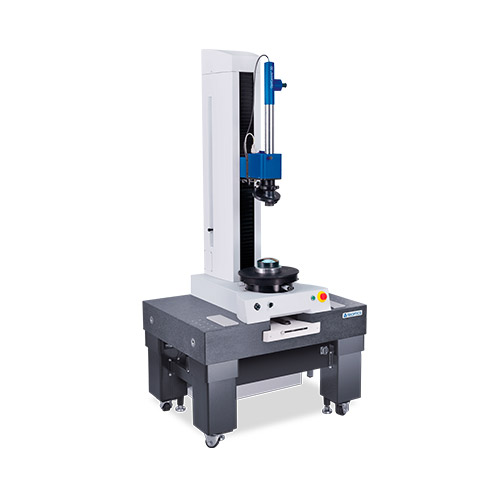
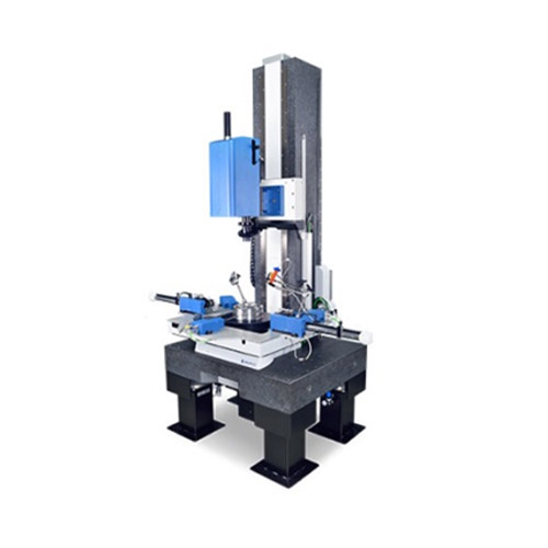
During set-up of these high-precision lens assemblies, the individual lens elements are aligned both to their cell and to one another with the aid of centration testing.
Validation of the image quality takes place through an MTF or wave front test.
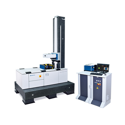
The size of the optics makes it especially difficult to change between the different measuring systems. For this reason, the integration of measuring systems in an efficient working process is extremely important.

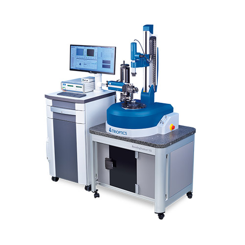
Bond and test precision optics highly accurately with five degrees of freedom
Precise alignment and bonding of large and heavy lenses in a cell